KiCAD PCB Design For Embedded Systems & Electronics Projects
- Description
- Curriculum
- FAQ
- Reviews
This course will help you to know the basics of KiCAD and how to use it as a tool for PCB design projects. And it’ll also teach you how to formulate a project/product idea and document it in such a way that it becomes easier for you to plan and design each part of the complete system.
And ultimately, help you develop a systematic way to approach PCB hardware design projects. Both as a hobbyist or as an engineering student. This course is Project-Based. You’ll learn KiCAD by doing practical project examples through this course.
Design 3 PCB Boards and Learn The Essentials of KiCAD
-
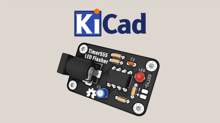
Simple LED Flasher Board
-
PIC18F-Based Development Board
-
STM32-Based USB-Powered LED Controller Board
Course’s Contents and Overview
The course starts with an introduction to printed circuit boards (PCB) technology. And then shifts the attention to PCB design CAD software tools and mainly focusing on KiCAD which is the main topic of this course. Then, you’ll get introduced to KiCAD tools for schematic capture and PCB layout editing through a very basic example board.
Afterward, I’ll teach you a very intuitive PCB design methodology to get any project done just in 10 actionable steps. And we’ll be sticking to this methodology for all the project examples we’ll be doing thereafter.
Then, the last 3 sections will be dedicated to the 3 projects for this course. And in each one of them, we’ll be doing:
-
HW Req. Statement
-
Schematic Design
-
Schematic Capture
-
ERC Check
-
Footprints Assignment
-
PCB Layout & Routing
-
DRC Check
-
Generating Fab.-Ready Output Files (Gerber)
-
Generating BOM File
-
Generating POS For SMT services
You’ll learn when and how to do each step in detail through this course and three times in 3 different projects. Just to make sure you’ve got a very good understanding and vision for the PCB design workflow.
Enjoy The Course!
-
5About KiCAD & Download and Install The SoftwareVideo lesson
-
6Create a New KiCAD ProjectVideo lesson
-
7Schematic Capture With KiCAD Eschema BasicsVideo lesson
-
8PCB Layout & Design With KiCAD BasicsVideo lesson
-
9Generating Fabrication-Ready Output Files (Gerber)Video lesson
-
10Create Your First KiCAD PCB ProjectText lesson
-
15Step1 - Hardware RequirementsVideo lesson
-
16Step2 - TLD DesignVideo lesson
-
17Step3 - Schematic DesignVideo lesson
-
18Step4 - Schematic CaptureVideo lesson
-
19Step5 - Footprints AssignmentsVideo lesson
-
20Step6 - ERC CheckVideo lesson
-
21Step7 - PCB Layout EditingVideo lesson
-
22Step8 - PCB RoutingVideo lesson
-
23Step9 - DRC CheckVideo lesson
-
24Optional Step - Silkscreen Custom Graphics DesignVideo lesson
-
25Step10 - Generating Fabrication-Ready Output Files (Gerber)Video lesson
-
26Step1 - Hardware RequirementsVideo lesson
-
27Step2 - TLD DesignVideo lesson
-
28Step3 - Schematic DesignVideo lesson
-
29Step4 - Schematic CaptureVideo lesson
-
30Step5 - Footprints AssignmentsVideo lesson
-
31Step6 - ERC CheckVideo lesson
-
32Step7 - PCB Layout EditingVideo lesson
-
33Step8 - PCB RoutingVideo lesson
-
34Step9 - DRC CheckVideo lesson
-
35Step10 - Generating Fabrication-Ready Output Files (Gerber)Video lesson
-
36Running Some Projects On PIC18F Dev BoardVideo lesson

External Links May Contain Affiliate Links read more


