Fundamentals of PN Junction Diode

- Description
- Curriculum
- FAQ
- Reviews
Dear Learners
Are you Preparing for Interview in Electronics? Don’t be stressed, take our PN Junction Diode Course and prepare yourself for your Interview
We know that PN junction diode is the most basic form of semiconductor device and its technology forms the basis of many other semiconductor devices. PN Junction diode is a basic component in electronics, so it is necessary for every students that he learn the Basic Concept of PN Junction Diode. In this Course You Will Learn the fundamentals of PN Junction Diodes and take the first leap to the world of Electronics.
This Course will Covers following topics:
-
Why PN Junction Diode is so Important in Electronics ?
-
PN Junction diode Structure
-
Forward Biasing & Reverse Biasing of PN Junction diode
-
PN-diode: current components under different biasing
-
I-V characteristics of PN Junction Diode
-
Breakdown Mechanism
-
Temperature Effect
-
Diode Approximation
-
Load Line Analysis for a PN Junction diode
-
Important terms used for a PN Junction diode
What is the Importance of PN Junction Diode ?
After resistor, capacitor and Inductor one of the most widely used electronic components is the PN junction diode. The PN junction diode is the basic semiconductor Component. It is used for many forms of rectification for current levels both large and small, as well as high and low voltage levels, and this semiconductor device finds many uses in all manner of electronic circuit designs. The PN junction has the very useful property that electrons are only able to flow in one direction. As current consists of a flow of electrons, this means that current is allowed to flow only in one direction across the structure, but it is stopped from flowing in the other direction across the junction. PN junction diodes can be obtained in a number of semiconductor materials – the earliest diodes tended to be made from germanium, but most of them today are silicon diodes.
In This Course we explain every topic in Simple and Easy Way, Definitely You Enjoy this Course.
Sign up now and take this Course. Let’s get started.
-
2
 Why P-N Junction Diode
Why P-N Junction Diode
PN junction diode is nonlinear circuit elements and many signal processing function
need it e.g. signal rectification .
PN junction is an important semiconductor device in itself and used in a wide variety
of applications such as rectifiers, Clipper and Clamper circuits, Photo detectors, light
emitting diodes (LED) and laser diode (LD) etc.
PN junctions are an integral part of other important semiconductor devices such as
BJTs, JFETS and MOSFETs.
P-N Junction
When a p-type semiconductor is brought in contact with n-type semiconductor, the
contact surface is called p-n junction.
Diffusion of electrons and holes from majority carrier side to minority carrier side
until drift balances diffusion.
-
3
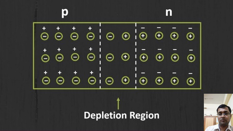
Construction of P-N Junction Diode
Region near to the p and n junction depleted from free carriers because of the
majority carriers diffusion ( leaving only fixed –ve and +ve ions in p and n region
respectively).
This internal electric field produces built-in-potentail which gives rise to the drift
current to the minority carriers and balances the diffusion current.
-
4
Forward Biasing & Reverse Biasing of P-N Junction diode
Forward Biasing of P-N Junction diode
A p-n Junction is said to be in Forward Bias when the P-type region is made positive
with respect to the N-type region.
Reverse Biasing of P-N Junction diode
A p-n Junction is said to be in Reverse Bias when the P-type region is made negative
with respect to the N-type region.
-
5
P-N Junction Diode: current components under different biasing
See the direction and magnitude of of drift current carefully. Drift current almost remains constant as it depends mainly on number of minority carriers
-
6
I-V characteristics of PN Junction Diode
Rapid increase in ID when reverse bias voltage exceeds a break down voltage VZ Breakdown mechanism is either Avalanche or Zener
-
7
Breakdown Mechanism
Avalanche break down:-
If both p-side and n-side of the diode are lightly doped, depletion region at the
junction widens. Application of a very large electric field at the junction may rupture
covalent bonding between electrons. Such rupture leads to the generation of a large
number of charge carriers resulting in avalanche multiplication.
In avalanche breakdown, VZ increases with temperature.
Zener break down:-
Breakdown Mechanism:
If both p-side and n-side of the diode are heavily doped, depletion region at the
junction reduces. Application of even a small voltage at the junction ruptures
covalent bonding and generates large number of charge carriers. Such sudden
increase in the number of charge carriers results in zener mechanism.
In Zener breakdown, VZ decreases with temperature
If the maximum specified power dissipation is not exceeded, breakdown is not
a destructive process.
-
8
Temperature Effect in PN Junction Diode
In the forward bias region, the characteristics of Si diode shift to the left
(lower voltage) at a rate of 2.5mV/oC increase in temperature.
Reverse saturation current is approximately doubles for every 10oC rise
in temperature. If Is= Is1 at T = T1, then at temperature T2, Is2 is given by,
I = I x 2(T –T )/10
-
9
PN Junction Diode Approximation
Diode Approximation:
Ideal diode
When diode is forward biased, resistance offered is zero, When it is reverse biased resistance offered is infinity. It acts as a perfect switch
2nd approximation:
const. voltage drop model
When forward voltage is more than 0.7 V, for Si diode then it conducts and offers zero resistance. The drop across the diode is 0.7V. When reverse biased it offers infinite resistance.
3rd approximation:
Piecewise linear model
When forward voltage is more than 0.7 V, for Si diode then it conducts and offers resistance. When reverse biased it offers very high resistance but not infinity.
-
10
Load Line Analysis for a p-n junction diode
The straight line represented by the above equation is known as the load line.
The load line passes through two points, I = 0, VD = V and VD= 0, I = V / RL.
The intersection point of load line and diode characteristics curve gives the
operating point.
-
11
Important terms used for a PN Junction Diode
Important terms used for a p-n junction diode:
Breakdown Voltage: It is the minimum voltage at which p-n junction breaks down with sudden rise in reverse current.
Knee Voltage: It is the forward voltage at which the current through the junction starts to increase rapidly.
Maximum forward Current: It is the highest instantaneous forward current that a p-n junction can conduct without damage to the junction .
Peak Inverse voltage (PIV): It is the maxium reverse voltage that can be applied to the p-n junction without damage to the junction .
Maximum power rating: It is the maximum power that can be dissipated at the junction without damaging it.
If the maximum specified power dissipation is not exceeded, breakdown is not a destructive process.
-
12
 QUIZ
QUIZ