PCB Designing in Altium Designer

- Description
- Curriculum
- FAQ
- Reviews
In this course, you will learn
1. The basic elements of a Printed Circuit Board.
2. The need for PCB and evolution of the same.
3. Steps involved in fabrication of a PCB
4. Steps involved in the design of a PCB
5. Types of PCB
6. Mounting Technologies – PTH, SMT
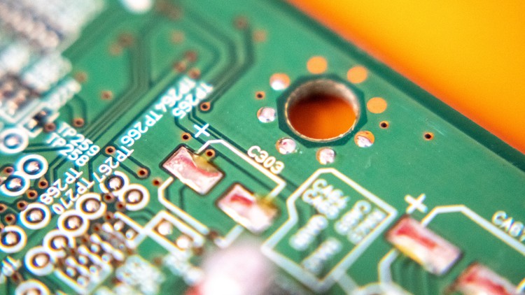
We will understand that PCB is a circuit board that connects all the electrical and electronic components through copper conductive tracks. The copper conductive tracks are embedded on a substrate which is basically a fiber.
After that, we will get into the Altium Designer Software in order to learn how to design a Printed Circuit Board.
1. Learning how to create a schematic and a PCB in the Altium Designer.
2. Understanding all the widgets and tools in the software.
3. Understanding how to route the footprints in a PCB – Both Manual and Auto Routing.
4. Analyzing the morphology of holes and solder pads.
5. Printing the texts in Top Overlay.
6. Creating libraries for two or three terminal components.
7. Creating libraries for some standard IC’s.
8. Getting the 2D and 3D Layouts of the PCB.
At the end of this course, you will be able to design a PCB in Altium Designer for your circuit knowing all the fundamentals of a Printed Circuit Board.